
Printed circuit boards are the backbone of all electronic devices. They provide the platform for circuit components to interact and produce the desired results. They help make gadgets smaller by reducing the need for bulky wires. Instead, they use flat copper traces to route power and electrical signals. If you are curious about the PCB manufacturing process, then read on to learn about the basics.
Design
It all starts from the circuit design which usually takes place on a PCB software. Engineers can simply drag and drop the elements that they need from a long list of predefined items. They can play with the positioning and test the circuit virtually for errors. This is faster, easier, and cheaper than doing it by hand. Optimizations can follow.
Once the design has been finalized, it will be printed on a clear sheet of film using a highly precise laser printer. When creating boards with multiple layers, it is prudent to include holes that can be used for alignment. These days, the files are usually sent to PCB manufacturers so that they can take over from there.
Expose
Untouched PCBs are laminate boards with copper covering the entire surface. Manufacturers need to remove the unwanted copper such that only the necessary traces remain intact. Many will use UV light exposure to accomplish this. The copper surface is cleaned and covered with light-sensitive film. Ultraviolet rays will not penetrate the black ink on the transparent sheet. Thus, the film will harden to cover the copper traces only. The rest will be removed.
Etch
The board will then be submerged in a chemical that can dissolve the copper from unprotected areas. The traces will remain thanks to the hardened film. The length of the chemical bath will depend on the thickness of the copper, the spacing of the tracks, and other factors. Once finished, the film will have to be washed off with a solvent. A thorough inspection will reveal flaws for correction.
Drill
Holes can now be placed where components need to go. For example, chips will need to have ample holes to accommodate all of their legs. These need to be clean, careful, and precise so a computer-controlled machine usually does the job for large manufacturers.
Silkscreen
PCBs can be incredibly complex such that even seasoned technicians and designers can get confused from going over them. Printing labels at various points can help in identifying what certain sections are for. These make design and troubleshooting easier.
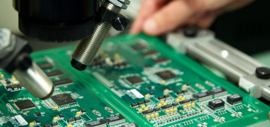
Test
Finally, technicians will perform electrical tests to make sure that the PCBs made comply to their standards and the original design. This can be automated for faster processing. Sometimes it may be necessary to cut the board so that it fits with the design of the device that it is supposed to inhabit.
Look for a reputable PCB manufacturing company that can do all of these so that you will not have to worry about them. Just send the files and get the finished product.